- 您现在的位置:买卖IC网 > Sheet目录511 > SI4972DY-T1-GE3 (Vishay Siliconix)MOSFET N-CH DUAL 30V 8-SOIC
Si4972DY
Vishay Siliconix
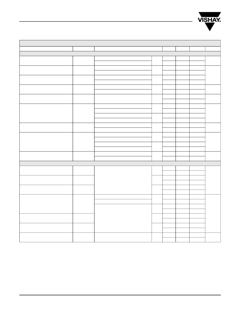
SPECIFICATIONS T J = 25 °C, unless otherwise noted
Parameter
Symbol
Test Conditions
Min.
Typ. a
Max.
Unit
Static
Drain-Source Breakdown Voltage
V DS Temperature Coefficient
V GS(th) Temperature Coefficient
V DS
Δ V DS /T J
Δ V GS(th) /T J
V GS = 0 V, I D = 250 μA
V GS = 0 V, I D = 250 μA
I D = 250 μA
I D = 250 μA
I D = 250 μA
I D = 250 μA
Ch 1
Ch 2
Ch 1
Ch 2
Ch 1
Ch 2
30
30
35
35
- 6.5
- 6.5
V
mV/°C
Gate Threshold Voltage
Gate-Body Leakage
V GS(th)
I GSS
V DS = V GS , I D = 250 μA
V DS = V GS , I D = 250 μA
V DS = 0 V, V GS = ± 20 V
Ch 1
Ch 2
Ch 1
Ch 2
1.5
1.5
3.0
3.0
100
100
V
nA
V DS = 30 V, V GS = 0 V
Ch 1
1
Zero Gate Voltage Drain Current
I DSS
V DS = 30 V, V GS = 0 V
V DS = 30 V, V GS = 0 V, T J = 55 °C
Ch 2
Ch 1
1
10
μA
V DS = 30 V, V GS = 0 V, T J = 55 °C
Ch 2
10
On-State Drain Current b
I D(on)
V DS = 5 V, V GS = 10 V
V DS = 5 V, V GS = 10 V
V GS = 10 V, I D = 6 A
Ch 1
Ch 2
Ch 1
10
10
0.012
0.0145
A
Drain-Source On-State
Resistance b
R DS(on)
V GS = 10 V, I D = 4.5 A
V GS = 4.5 V, I D = 5.6 A
Ch 2
Ch 1
0.022
0.016
0.0265
0.0195
Ω
V GS = 4.5 V, I D = 4 A
Ch 2
0.030
0.036
Forward Transconductance b
g fs
V DS = 15 V, I D = 6 A
V DS = 15 V, I D = 4.5 A
Ch 1
Ch 2
27
20
S
Dynamic a
Input Capacitance
C iss
Channel 1
Ch 1
Ch 2
1080
515
Output Capacitance
Reverse Transfer Capacitance
Total Gate Charge
C oss
C rss
Q g
V DS = 15 V, V GS = 0 V, f = 1 MHz
Channel 2
V DS = 15 V, V GS = 0 V, f = 1 MHz
V DS = 15 V, V GS = 10 V, I D = 5 A
V DS = 15 V, V GS = 10 V, I D = 5 A
Ch 1
Ch 2
Ch 1
Ch 2
Ch 1
Ch 2
Ch 1
170
91
72
38
18.5
9.6
8.3
28
15
13
pF
Gate-Source Charge
Gate-Drain Charge
Gate Resistance
Q gs
Q gd
R g
Channel 1
V DS = 15 V, V GS = 4.5 V, I D = 5 A
Channel 2
V DS = 15 V, V GS = 4.5 V, I D = 5 A
f = 1 MHz
Ch 2
Ch 1
Ch 2
Ch 1
Ch 2
Ch 1
Ch 2
4
3.9
1.9
2.7
1.3
2.5
2.9
6
3.8
4.4
nC
Ω
www.vishay.com
2
Document Number: 73849
S09-0138-Rev. D, 02-Feb-09
发布紧急采购,3分钟左右您将得到回复。
相关PDF资料
SI4973DY-T1-GE3
MOSFET 2P-CH 30V 5.8A 8SOIC
SI5040-D-GM
IC TXRX XFP 10GBPS 32LGA
SI5402DC-T1-GE3
MOSFET N-CH D-S 30V 1206-8
SI5403DC-T1-GE3
MOSFET P-CH 30V 6A 1206-8
SI5432DC-T1-GE3
MOSFET N-CH 20V 6A 1206-8
SI5440DC-T1-GE3
MOSFET N-CH D-S 30V 1206-8
SI5441DC-T1-GE3
MOSFET P-CH D-S 20V 1206-8
SI5443DC-T1-GE3
MOSFET P-CH D-S 20V 1206-8
相关代理商/技术参数
SI4973DY
制造商:Vishay Intertechnologies 功能描述:Trans MOSFET P-CH 30V 5.8A 8-Pin SOIC N
SI4973DY-T1
制造商:Vishay Intertechnologies 功能描述:Trans MOSFET P-CH 30V 5.8A 8-Pin SOIC N T/R
SI4973DY-T1-E3
功能描述:MOSFET P-CHANNEL 25V RoHS:否 制造商:STMicroelectronics 晶体管极性:N-Channel 汲极/源极击穿电压:650 V 闸/源击穿电压:25 V 漏极连续电流:130 A 电阻汲极/源极 RDS(导通):0.014 Ohms 配置:Single 最大工作温度: 安装风格:Through Hole 封装 / 箱体:Max247 封装:Tube
SI4973DY-T1-GE3
功能描述:MOSFET 30V 7.6A 2.0W 23mohm @ 10V RoHS:否 制造商:STMicroelectronics 晶体管极性:N-Channel 汲极/源极击穿电压:650 V 闸/源击穿电压:25 V 漏极连续电流:130 A 电阻汲极/源极 RDS(导通):0.014 Ohms 配置:Single 最大工作温度: 安装风格:Through Hole 封装 / 箱体:Max247 封装:Tube
SI4974DY-T1-E3
功能描述:MOSFET DUAL N-CH 30V(D-S) RoHS:否 制造商:STMicroelectronics 晶体管极性:N-Channel 汲极/源极击穿电压:650 V 闸/源击穿电压:25 V 漏极连续电流:130 A 电阻汲极/源极 RDS(导通):0.014 Ohms 配置:Single 最大工作温度: 安装风格:Through Hole 封装 / 箱体:Max247 封装:Tube
SI4980DY
功能描述:MOSFET 80V 3.7A 2W RoHS:否 制造商:STMicroelectronics 晶体管极性:N-Channel 汲极/源极击穿电压:650 V 闸/源击穿电压:25 V 漏极连续电流:130 A 电阻汲极/源极 RDS(导通):0.014 Ohms 配置:Single 最大工作温度: 安装风格:Through Hole 封装 / 箱体:Max247 封装:Tube
SI4980DY-E3
功能描述:MOSFET 80V 3.7A 2W RoHS:否 制造商:STMicroelectronics 晶体管极性:N-Channel 汲极/源极击穿电压:650 V 闸/源击穿电压:25 V 漏极连续电流:130 A 电阻汲极/源极 RDS(导通):0.014 Ohms 配置:Single 最大工作温度: 安装风格:Through Hole 封装 / 箱体:Max247 封装:Tube
SI4980DY-T1
功能描述:MOSFET 80V 3.7A 2W RoHS:否 制造商:STMicroelectronics 晶体管极性:N-Channel 汲极/源极击穿电压:650 V 闸/源击穿电压:25 V 漏极连续电流:130 A 电阻汲极/源极 RDS(导通):0.014 Ohms 配置:Single 最大工作温度: 安装风格:Through Hole 封装 / 箱体:Max247 封装:Tube
